
- Description
- Inquiry
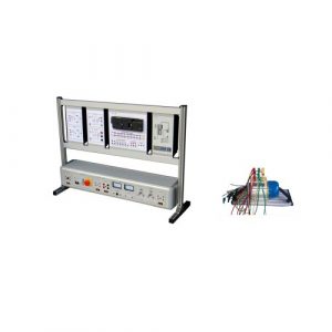
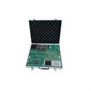
TB230621S07 FPGA Innovative Development Training Kit Teaching Equipment Electrical Engineering Lab Equipment
Product description
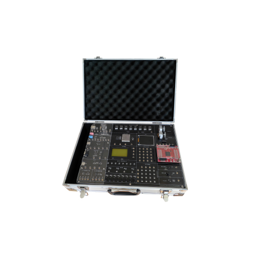
Digital logic (FPGA) design innovation development experiment box is a new experimental platform developed by our company to meet the development of electronic technology. The experimental platform is rich in hardware resources, it can meet the requirements of students
major in electronic communication to complete the digital logic design course experiment, innovation and development experiment, and the engineering actual algorithm training needs. The platform is equipped with an extensible interface to customize industry specific modules. And the platform performance is stable and cost-effective.
Product composition
| No.
| Item name | Quantity | Remarks |
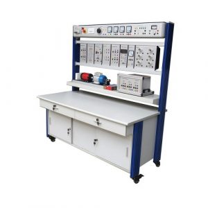
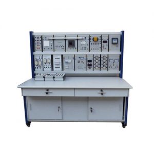
| 1 | Digital Logic (FPGA) Innovative Development Experiment Box | 1set
| RZ9657 |
| 2 | Multimeter | 1pcs | Self-preparation |
| 3 | Double trace digital oscilloscope | 1pcs | Self-preparation |
| 4 | PC | 1set | Self-preparation |
| 5 | JTAG download line | 1pcs |
Technical parameters
- The experiment box adopts the main board plus module structure, and the connector is reliable and easy to upgrade and maintain.
- FPGA adopts EP4CE22, optional host network port loading, host USB port loading.
- Display module: 12864 LCD module, TFT color hydraulic crystal module, LED based on SPI bus.
- Signal module: Generate various signal sources based on STM32F4. 5. Memory module SD card module, I2C bus FLASH, SPI bus (X25045). 6. Modulus and digital-analog conversion module: AD7888, DAC5311. 7. Voice Interface Module: WM8731.
- Communication interface module: Network port, USB port.
- Motor measurement and control module: Stepper motor, photoelectric speed measurement.
- Communication extension module: High speed AD/DA, conversion rate is not less than 200MSPS. Basic experiments
Basic gate circuit and trigger:
- Basic Gate Circuit
- Basic trigger
- 3-8 Decoder
- 8-3 Encoder
- BCD eight-segment display decoder
- Four selection one data selector
- Numerical value Comparator
- 4-bit binary adder
- 4-bit binary multiplier
Logic circuit
- Shift register
- Serial and parallel conversion
- Single clock synchronous reversible counter
- Sequence pulse generation and detection
- Key digital tube circulatory left shift display
- Electronic clock
- Key control
FPGA comprehensive application
- Digital coded lock
- Intelligence responder
- Vending machine
- Digital frequency meter
SOPC system development
- Building a Qsys environment based on FPGA
- IO port operation based on Qsys
- USB communication based on Qsys
- SD card reading and writing based on Qsys
- AD conversion based on Qsys
- DA conversion based on Qsys
- LCD display based on Qsys (12864 dot matrix and TFT color)
- network interface based on Qsys
- Voice interface based on Qsys (WM8731)
- Comprehensive test based on Qsys
Related Products
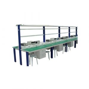
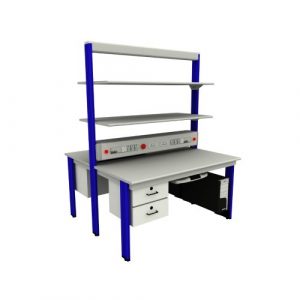
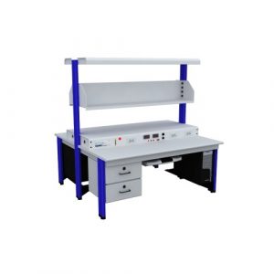
ZE1107 Electronics Workbench Educational Stand
ZE1107 Electronics Workbench Educational Stand. Jinan Should Shine Didactic Equipment Co., Ltd. is company specialized in manufacture and trading Engineering Educational Equipment,Technical Teaching Equipment, Vocational Training Equipment, Didactic Equipment for university,college, technical institution, polytechnics.Should Shine products has been exported to America,Asia,Europe, Africa, Australia.
ZE3108F PLC Trainer With Motor Teaching Equipment
ZE3108F PLC Trainer With Motor Teaching Equipment for university,college,technical institution,vocational training schools.
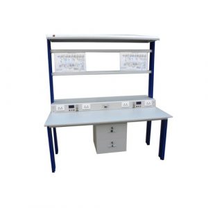
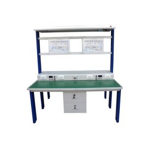
ZE1105 Electronics Workbench Educational Training Equipment
ZE1105 Electronics Workbench Educational Training Equipment
Jinan Should Shine Didactic Equipment Co., Ltd. is company specialized in manufacture and trading Engineering Educational Equipment,Technical Teaching Equipment, Vocational Training Equipment, Didactic Equipment for university,college, technical institution, polytechnics.Should Shine products has been exported to America,Asia,Europe, Africa, Australia.
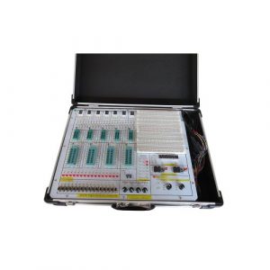
ZE3161 Digital Educational Kit Vocational Training Equipment
ZE3161 Digital Educational Kit Vocational Training Equipment for university,college,technical schools,technical institute, vocational training schools.
ZE1109 Electronics Educational Equipment Teaching Equipment
ZE1109 Electronics Educational Equipment Teaching Equipment Jinan Should Shine Didactic Equipment Co., Ltd. is company specialized in manufacture and trading Engineering Educational Equipment,Technical Teaching Equipment, Vocational Training Equipment, Didactic Equipment for university,college, technical institution, polytechnics.Should Shine products has been exported to America,Asia,Europe, Africa, Australia.
SR2112S Power Electronics Trainer Didactic Equipment
Power Electronics Trainer Didactic Equipment for college,university,technical institute,vocational schools.
ZE4199 AC Circuit Trainer Vocational Training Equipment
ZE4199 AC Circuit Trainer Vocational Training Equipment. Jinan Should Shine Didactic Equipment Co., Ltd. is company specialized in manufacture and trading Engineering Educational Equipment,Technical Teaching Equipment, Vocational Training Equipment, Didactic Equipment for university,college, technical institution, polytechnics.Should Shine products has been exported to America,Asia,Europe, Africa, Australia.
ZE1108 Technical Teaching Equipment Electronics Workbench
ZE1108 Technical Teaching Equipment Electronics Workbench. Jinan Should Shine Didactic Equipment Co., Ltd. is company specialized in manufacture and trading Engineering Educational Equipment,Technical Teaching Equipment, Vocational Training Equipment, Didactic Equipment for university,college, technical institution, polytechnics.Should Shine products has been exported to America,Asia,Europe, Africa, Australia.
ZE2101 Vocational Training Equipment
ZE2101 Vocational Training Equipment. Jinan Should Shine Didactic Equipment Co., Ltd. is company specialized in manufacture and trading Engineering Educational Equipment,Technical Teaching Equipment, Vocational Training Equipment, Didactic Equipment for university,college, technical institution, polytechnics.Should Shine products has been exported to America,Asia,Europe, Africa, Australia.
ZE1106 Electronics Workbench Technical Educational Equipment
ZE1106 Electronics Workbench Technical Educational Equipment. Jinan Should Shine Didactic Equipment Co., Ltd. is company specialized in manufacture and trading Engineering Educational Equipment,Technical Teaching Equipment, Vocational Training Equipment, Didactic Equipment for university,college, technical institution, polytechnics.Should Shine products has been exported to America,Asia,Europe, Africa, Australia.